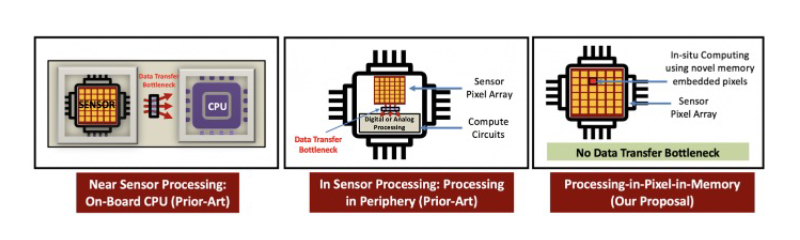
In recent decades, smart sensing technology has undergone considerable evolution to meet performance demands and address resource limitations in edge devices. This evolution has shifted from traditional separate Sensor-NPU-CPU architectures [1-2] to in-sensor processing [3]. However, data movement between the sensor and peripheral logic continues to incur substantial energy and bandwidth costs. With the increasing deployment of AI on edge devices, lightweight neural networks for tasks like object classification, eye tracking, and hand gesture recognition are becoming viable for intelligent devices. For energy-sensitive applications such as smart rings and wearable glasses, an energy-efficient sensing system is crucial.
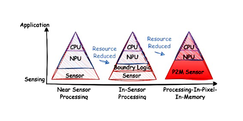
Therefore, the research group from UW-Madison ECE led by Assistant Prof. Akhilesh Jaiswal proposed the P2M paradigm, which enables processing-in-pixel-in-memory [4]. In collaboration with Prof. Umit Yusuf Ogras, an integral SoC imaging system was designed and verified. This system features a P2M-based sensing front-end and minimizes resource overhead for completing the entire neural network using the small data output from the P2M sensor array. The design was sign-off verified in GF 22nm technology on May 1st. This approach enables the initial layers of sensing and computation to be completed directly within the sensor array, eliminating the need to transfer data to off-sensor boundary logic. The trained weights for these first few network layers are mapped to specific transistor sizes within the pixel array. This design choice does not compromise the feasibility of downstream applications because the initial layers of modern CNNs typically function as high-level feature extractors, which are common across numerous vision tasks. As Fig. 1 depicts, relocating a portion of the neural network computation to the sensor array effectively reduces the area and power overhead associated with a standalone NPU, thereby easing the demands for NPU.
The P2M pixel array significantly advances deep learning hardware by embedding critical Convolutional Neural Network (CNN) functionalities directly within each pixel’s architecture. As detailed in Fig. 2, each pixel is meticulously designed to support analog multi-channel, multi-bit convolution, along with crucial operations like batch normalization and ReLU. During a convolution operation, only one weight transistor (Wi) within a pixel is activated at any given time. This transistor corresponds to a specific input channel and, through its driving strength, effectively represents the multi-bit weight for that channel. The pixel’s inherent photosensitivity means that the photodiode current provides the input activation. This current is then analogously modulated by the activated Wi transistor, performing the essential multiplication step of the convolution. The output of this analog computation is then manifested as a voltage on the bit lines, which directly represents the convolution result. To achieve high throughput, the system can concurrently activate a large number of pixels, specifically X×Y×3 pixels. Here, X and Y represent the spatial dimensions of the input, and ‘3’ refers to the RGB (red, green, blue) color channels, enabling efficient parallel processing of image data.
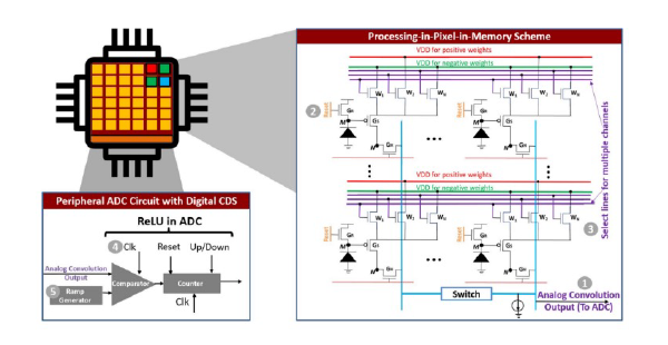
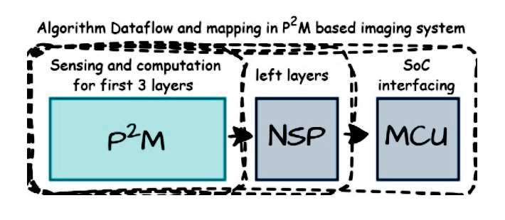
Fig. 3 illustrates the complete algorithm flow and module mapping for a P2M based imaging system. Beyond the P2M block, the inferencing model incorporates a near-sensor processing (NSP) module for the remaining neural network layers and an MCU equipped with robust co-processing communication and interrupt capabilities. The heterogeneous integration of P2M imaging system enables direct processing of raw sensor data into an extracted feature map, ready for downstream tasks. By verification on the VWW [5] dataset, the P2M-enabled custom model significantly reduces computational demands. It cuts Multiply-Accumulate operations (MAdds) by approximately 7.15× and peak memory usage by about 25.1× for 560 × 560 image resolution. This comes with a minimal 1.47% drop in test accuracy compared to the uncompressed baseline model. This substantial memory reduction allows our P2M model to even run on tiny microcontrollers with just 270KB of on-chip SRAM. While both baseline and custom model accuracies decrease with reduced image resolution (with a more notable drop for the custom model), this highlights the importance of high-resolution images for optimal performance.
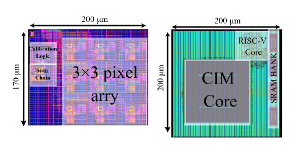
Comparing standard models with P2M -implemented counterparts reveals significant energy efficiencies. Specifically, P2M can reduce energy consumption by up to 7.81×. This energy saving becomes even more pronounced when feature maps would otherwise need to be transferred from an edge device to the cloud for further processing, largely due to high communication overheads. Based on simulation verification from reference [4], a full silicon design has been launched in GF22nm technology. This design incorporates separate components, including the calibration module, re-purposes correlated double sampling (CDS) circuit and single slope ADC (SS-ADC) and a 3 × 3 pixel array. In parallel, a SoC for future integration, managing the remaining neural network layers outside the P2M block with minimal memory overhead, has also been implemented within the same GF 22nm shuttle. This push toward heterogeneous integration, particularly for energy and resource-constrained scenarios, aims to realize a truly intelligent edge-computing paradigm, evolving from novel sensing architectures to advanced AI-driven devices.