Originally posted on August 28, 2025, by Jason Daley
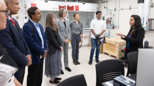
It’s not unusual for highly advanced research labs to open across the University of Wisconsin-Madison campus. But on Aug. 5, 2025, a host of researchers, administrators and industry representatives gathered in the Engineering Centers Building to celebrate one particularly impressive lab. The Ultra-Wide Bandgap Semiconductor Metal-Organic Chemical Vapor Deposition (MOCVD) Laboratory is a unique research space that gives UW-Madison capabilities rarely found on university campuses.
Among university and national R&D leaders at the lab’s grand opening were UW-Madison’s vice chancellor for research, Dorota Grejner-Brzezinska; College of Engineering Dean Devesh Ranjan; and Vivek Prasad, vice president for design engineering ecosystem enablement at NatCast, a nonprofit that operates the National Semiconductor Technology Center. They joined Susan Hagness, chair of the Department of Electrical and Computer Engineering and ECE Assistant Professor Shubhra Pasayat, who oversees the new facility as the lab’s principal investigator.
The facility will serve as the cornerstone of the College of Engineering-led focus at UW-Madison on an emerging class of materials called III-nitride semiconductors, which are at the heart of dozens of next-gen technologies. “These semiconductors have uses in all sorts of applications,” says Pasayat. “Deep ultraviolet LEDs; high-power radar; high-voltage power electronics, motors, and vehicles; as well as nuclear reactors and applications in other extreme conditions like space.”
For the last 70 years, silicon-based semiconductors have been the core of the electronics industry. Not only are integrated circuits made of silicon wafers and transistors the brains of most computers, they are also the foundation of communications chips, opto-electronics like LEDs and lasers, and the power electronics that regulate and convert the electricity in our electronic gadgets and electric motors.
While these technologies have become smaller and more powerful, silicon is unfortunately reaching its fundamental material limits: it can no longer handle the high energy, frequencies and temperatures required for next-generation technologies. That’s why researchers have turned their attention to “wide bandgap” semiconductors, like silicon carbide and gallium nitride—a III-nitride material—that can handle much higher voltages than silicon.
Wide bandgap semiconductors allow for smaller, faster, more efficient electronic devices that can handle much higher energies and frequencies. The electronics industry is already rapidly adopting these semiconductors for use in fast chargers, radar systems, LED lighting and even microchips. As fabrication techniques improve and costs decrease, wide-bandgap semiconductors will become even more commonplace.
But researchers are already looking past these wide bandgap semiconductors to ultra-wide bandgap materials, including III-nitride semiconductors aluminum gallium nitride and aluminum nitride. These materials are even more robust, and able to survive conditions ranging from the extreme temperatures found in hypersonic jets to radiation in modular nuclear reactors. They can also handle the wide frequency switching in 6G communications and beyond, among other emerging uses.
At the moment, fabricating and characterizing these ultra-wide bandgap semiconductors is extremely challenging because they require expensive equipment and deep expertise in metal-organic chemical vapor deposition (MOCVD) or other advanced commercialization- friendly deposition techniques.
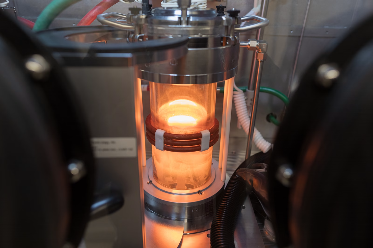
When she first joined UW-Madison in 2021, Pasayat set up a commercial Aixtron MOCVD reactor, which uses high temperatures and low pressure to convert gasses into thin layers of crystalline solids, including wide bandgap materials like gallium nitride and low-aluminum aluminum gallium nitride. This helped establish her at the forefront of wide bandgap semiconductor research.
Now, the new facility, which took years of planning and cooperation among UW-Madison, the College of Engineering and the Department of Electrical and Computer Engineering, takes that research to the next level. The newly installed Agnitron Agilis 100 system can handle even higher temperatures and lower pressures, allowing Pasayat and her students to design and precisely synthesize high-quality two-inch diameter wafers of high-aluminum content aluminum gallium nitride, aluminum nitride and other ultra-wide bandgap materials.
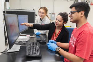
Pasayat says this capability is already opening up a huge number of collaborations with researchers across campus and is drawing industry partners to UW-Madison. It’s also an incredible opportunity for students, she says, who will enter the workforce trained on some of the most advanced fabrication equipment available and with hands-on knowledge of next-generation materials.
Pasayat’s lab is at the center of UW-Madison’s rising III-nitride ecosystem. The onsite faculty’s broad expertise in chip design and architecture, materials characterization, fabrication, advanced packaging, and systems integration means these ultra-wide bandgap semiconductors can go from the drawing board to the motherboard all on one campus—streamlining and improving the research process.
The new reactor cements UW-Madison’s reputation as a vibrant III-nitride research hub, Dean Ranjan told the crowd at the opening ceremony.
Pasayat says she is excited that her lab will have a central place in that development. ECE chair Hagness shares that enthusiasm. “This magnificent new facility represents a timely investment in not only supporting the research program of one of our innovative assistant professors, but also in accelerating the transition from academic research to commercial and societal outcomes on a national scale,” she says. “Under Professor Pasayat’s technical leadership, UW-Madison is positioned to be a global leader in innovations in III-nitride semiconductor materials”