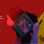
Wisconsin CHIPS joins SWAP Hub & ME Commons
Wisconsin CHIPS is pleased to announce its new membership to the Southwest Advanced Prototyping (SWAP) Hub led by Arizona State University. The SWAP Hub is one of eight that makes up the Microelectronics (ME) Commons, which was established to position the United States as a global leader in microelectronics research and enable domestic fabrication.
February 6, 2026
Kawasaki named a Moore Foundation Experimental Physics Investigator
Jason Kawasaki, an associate professor in materials science and engineering at the University of Wisconsin-Madison, has been named a 2025 Gordon and Betty Moore Foundation Experimental Physics Investigator. Selection to the program is a prestigious honor …
October 28, 2025
2025 Nobel Prize Laureate John Martinis’s Connections to UW–Madison
Wisconsin CHIPS congratulates the 2025 laureates of The Nobel Prize in Physics—John Clarke, Michel H. Devoret, and John M. Martinis—for observation of quantum-mechanical tunneling in an electrical circuit based on superconductors! Excitingly, Martinis has connections to UW–Madison through shared research and his co-founded company Qolab.
October 21, 2025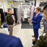
UW fostering closer research ties with federal defense, cybersecurity agencies
UW–Madison is building stronger research partnerships with federal defense and cybersecurity agencies to advance technologies that serve the public good. A recent campus visit from Department of Defense and NSA leaders highlighted shared priorities in AI, quantum computing, and secure systems.
October 20, 2025
With NSF CAREER Award, Chirag Gupta is using next-gen materials to engineer high performance power semiconductor transistors
Chirag Gupta earned an NSF CAREER Award to advance power semiconductor transistors using next-gen materials. His research could lead to more efficient, compact, and reliable electronics for energy, transportation, and communication systems.
October 16, 2025
With DARPA Young Faculty Award, Jacobberger will develop industry-ready diamond semiconductors
Jacob Berger received a DARPA Young Faculty Award to develop diamond-based semiconductors. His work aims to create high-performance, scalable materials for next-gen electronics in defense and commercial applications.
October 15, 2025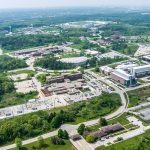
Exploring Decades of Semiconductor Collaboration between Argonne National Lab & UW–Madison
UW–Madison and Argonne National Laboratory have built a portfolio of shared research for decades. Read how semiconductor researchers from all interest areas have benefited from this affiliation.
October 10, 2025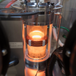
New facility establishes UW-Madison as a hub for next-generation semiconductors
UW–Madison has launched a state-of-the-art facility focused on ultra-wide bandgap semiconductors, positioning the university as a key player in next-generation chip research and industry collaboration.
September 17, 2025- More News